|
|
|
![[ Home ]](home1.gif) ![[ Introduction ]](intro1.gif) ![[ The Web ]](web1.gif) ![[ HTML ]](html1.gif) ![[ Bookmarks ]](links1.gif) ![[ Word ]](word1.gif) ![[ Excel ]](excel1.gif) ![[ Access ]](access1.gif) ![[ Tori Amos ]](tori1.gif) ![[ Robert Heinlein ]](heinlein1.gif) ![[ Jeff ]](jeff1.gif) |
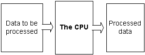
What is a CPU?The CPU is certainly the most important PC component.
CPU stands for Central Processing Unit. Let us briefly study that
name:
Speed, Speed, SpeedWithout the CPU, there would be no PC. Like all other hardware components, the CPUs are continually undergoing further development. You can see the explosive technological development in data processing most clearly in the development of newer and faster CPUs. The CPUs have for years doubled their performance about every 18 months ( Moore's Law ), and there are no indications that this trend will stop.When we now look at all the CPUs from a broader perspective, we can see that:
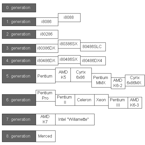
CPUs - brief reviewCPU history starts in 1971, when a small unknown company, Intel, for the first time combined multiple transistors to form a central processing unit - a chip called Intel 4004. However, it was 8 years before the first PC was constructed. PCs are designed around different CPU generations. Intel is not the only company manufacturing CPUs, but by far the leading one. The following table shows the different CPU generations. They are predominantly Intel chips, but in the 5th generation we see alternatives:
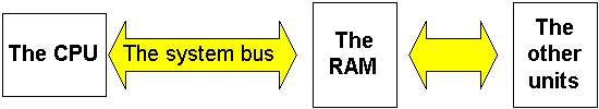
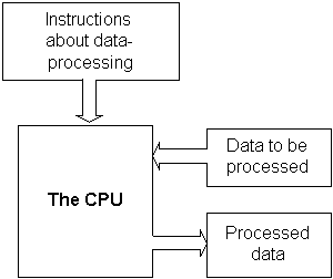
How does a CPU work?The CPU is centrally located on the motherboard. Since the CPU carries out a large share of the work in the computer, data pass continually through it. The data come from the RAM and the units (keyboard, drives etc.). After processing, the data is send back to RAM and the units. The CPU continually receives instructions to be executed. Each instruction is a data processing order. The work itself consists mostly of calculations and data transport:
Data have a path to the CPU. It is kind of a data expressway called the system bus.
Two types of dataThe CPU is fed long streams of data via the system bus. The CPU receives at least two types of data:
What we call instructions is program code. That includes those messages, which you continuously send to the PC from the mouse and keyboard. Messages to print, save, open, etc. Data are typically user data. Think about the letter, which you are
writing to Aunt Karen. The contents, letters, images, etc., are
user
data. but then you say "print," you are sending program code (instructions):
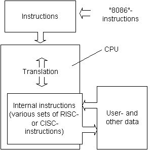
8086 compatible instructionsThe biggest job for the CPU consists of decoding the instructions and localizing data. The calculations themselves are not heavy work. The decoding consists of understanding the instructions, which the user program sends to the CPU. All PC CPUs, are "8086 compatible." This means that the programs communicate with the CPU in a specific family of instructions. These instructions were originally written for the Intel 8086 processor, which founded the concept "the IBM compatible PC." The 8086 from 1978 received its instructions in a certain format. Since there was a desire that subsequent CPU generation should be able to handle the same instructions which the 8086 could, it was necessary to make the instruction sets compatible. The new CPUs should understand the same instructions. This backwards compatability has been an industry standard ever since. All new processors, regardless of how advanced, must be able to handle the 8086 instruction format. Thus, the new CPUs must use much effort to translate the 8086 instruction format to internal instruction codes:
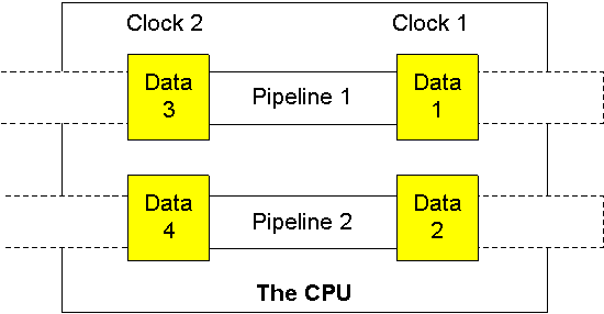
CISC and RISC instructions and their handlingThe first CPUs had a so called Complex Instruction Set Computer (CISC). This means that the computer can understand many and complex instructions. The X86 instruction set, with its varying length from 8 to 120 bit, was originally developed for the 8086 with its mere 29000 transistors. Reduced Instruction Set Computer (RISC)The RISC instructions are brief and the same length (for example 32 bit long, as in Pentium Pro), and they process much faster than CISC instructions. Therefore, RISC is used in all newer CPUs. However, the problem is that the instructions arrive at the CPU in 8086 format. Thus, they must be decodedFor every new CPU generation, the instruction set has been expanded. The 386 came with 26 new instructions, the 486 with 6 new instructions, and Pentium with 8 new instructions. These changes mean that some programs require at least a 386 or a Pentium processor to work. Dual pipeline: more work per clock strokeThere is also a continuous optimizing of the instruction handling process. One is that the clock frequency increases, as we will see later - the faster, the better. But what can the CPU do in one clock tick. That is critical to its performance. For example, a 386 needed 6 clock ticks to add a number to a sub total. A job which the 486 manages in only two clock ticks, because of more effective instruction decoding.5th and 6th generation CPUs can execute more than one of those operations in one clock tick, since they contain more processing lines (pipelines), which work parallel:
Floating point unit - FPUThe first CPUs could only work with whole numbers. Therefore, it was necessary to add a mathematical co-processor (FPU), when better math power was needed. Later, this FPU was built into the CPU:
It is said that Intel's CPUs have by far the best FPU units. Processors from AMD and Cyrix definitely have a reputation for providing sub standard performance in this area. But, you may not utilize the FPU. That depends on the applications (user programs) you are using. Common office programs do not use the floating point operations, which the FPU can handle. However, 3D graphics programs like AutoCad do. And all 3D-games like Quake rely heavily on FPU perfomance! Therefore, if you use your PC in advanced design applications, the FPU performance becomes significant. For some users, it is only of limited importance. Graphic overview of the processorsThere are CPUs of many brand names (IBM, Texas, Cyrix, AMD), and often they make models which overlap two generations. This can make it difficult to keep of track of CPUs. Here is an attempt to identify the various CPUs according to generation:
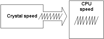
Clock frequencyWe know this from the ads: "A Celeron 466 MHz." The 466 MHz is the clock frequency. Actually, there is a small crystal on the motherboard. which continually ticks to the CPU at a steady number of clock ticks per second. At each clock tick something happens in the CPU. Thus, the more ticks per second the more data are processed per second.
The first CPUs worked at a frequency of 4.77 MHz. Subsequently then, clock frequencies rates rose to 16, 25, 50, 66, 90, 133 and 200 MHz to the best today, which operate at 550 MHz. Clock frequencies are still being increased. In a few years we will have CPUs operating at 1,200 MHz and more. To reach these very high clock frequencies, one has to employ a technique called clock doubling : Clock doubling in the CPUThe problem with the high clock frequencies is to ensure that other electronic components keep up with the pace. It is rather simple to make data move very fast inside a chip where the print tracks are microscopic. But when we move outside the chip, other problems appear. The other components must be able to keep up with the pace. When the frequency gets too high, the circuit board print tracks start acting as antennae and various forms of "radio noise" appears. Briefly, it becomes expensive to make the rest of the hardware to keep up with these high frequencies. The solution to this problem was to split the clock frequency in two:
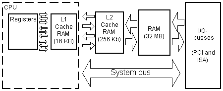
Intel's 80486DX2 25/50 MHz was the first chip with clock doubling. It was introduced in 1992 with great potential. For a lower price you could acquire a chip, which provided 90% of the 486DX50 performance. The DX50 ran at 50 MHz both internally and externally. The DX2 ran at just 25 MHz on the system bus. This enabled lower cost motherboards. Also RAM speed demands were lower. Clock doubling occurs inside the CPU. If the motherboard crystal works at 25 MHz, the CPU will receive a signal every 40 nanosecond (ns). Internally in the CPU, this frequency is doubled to 50 MHz. Now the clock ticks every 20 ns inside the CPU. This frequency governs all internal transactions, including integer unit, floating point unit, and all memory management unit operations as well as others. The only area still working at 25 MHz are external data transfers. That is transfers to RAM, BIOS and the I/O ports. Today the speed problem is in RAM. The ordinary FPM RAM and EDO RAM can function at a maximum of 66 MHz (possibly 75 MHz). Therefore, Pentium and similar CPUs were "clocked up" with factors from 2 to 5 internally. They work well at high frequencies like 166, 200, 233, 266, 300 and 333 MHz. In 1998 the PC100 RAM was introduced together with new motherboards and chip set. This RAM works at 100 MHz, and using the clock factors 3.5, 4 and 4.5 we have CPUs running at 350, 400 and 450 MHz. The Intel CPUs Pentium II, Celeron, and Pentium III can operate with clock factors of up to 8. With PC133 RAM this indicates clock frequencies up to 1066 MHz. About CPU cache RAMThe CPU must deliver its data at a very high speed. The regular RAM cannot keep up with that speed. Therefore, a special RAM type called cache is used as a buffer - temporary storage. To get top performance from the CPU, the number of outgoing transactions must be minimized. The more data transmissions, which can be contained inside the CPU, the better the performance. Therefore, the 486 was equipped with a built in mathematical co-processor, floating point unit and 8 KB L1-cache RAM. These two features help minimize the data flow in and out of the CPU. Cache RAM becomes especially important in clock doubled CPUs, where internal clock frequency is much higher than external. Then the cache RAM enhances the "horsepower" of the CPU, by allowing faster receipt or delivery of data. Beginning with 486 processors, two layers of cache are employed. The fastest cache RAM is inside the CPU. It is called L1 cache. The next layer is the L2 cache, which are small SRAM chips on the motherboard. See the illustration below of a traditional Pentium PC:
Cache overviewL1-cache first appeared in Intel's 80486DX chip. Today, bigger and better CPU cache is a natural step in the development of new CPUs:
Areas of developmentIn the following table, you see some of the technologies, which can be improved in the CPU design. Note that internal means inside the CPU. External speed, etc. refers to features immediately outside the CPU on the motherboard.
The CPU speed measurementWhen we look at a CPU, its speed is the most significant feature. All newer CPUs can do the same. You can run Office 2000 in Windows 98 on a 486 CPU. It would be quite slow, but it is possible. Speed is the primary difference between newer CPUs. Speed improvement is a product of the above mentioned technologies (such as clock frequency and bus width). There are many, many ways to measure CPU speed. The subject is boundless. For years, Norton's Speed Index has provided a good sounding board. That is a test, which can be run on any PC with the Norton Utilities Sysinfo program. In the table below, you see a number of the most common older CPUs. You can see how they are designed regarding clock speed and bus width. The last column shows their Norton Speed Index (SI). That is a relative number, which can be used to compare different CPUs. It is not used for modern CPUs.
Newer CPUs are compared by their clock frequency. CPU changes - historical reviewThis describes briefly the changes throughout the CPU generations: 8088 and 8086The 8086 from 1978 was the first 16 bit CPU from Intel using a 16 bit system bus. However 16 bit hardware such as motherboards were too expensive and even non existing at this time, where the 8 bit microcomputers were the standard.In 1979 Intel reengineered the CPU so it fit with existing 8 bit hardware. The first PC (in 1981) had this 8088 CPU. The 8088 is a 16 bit CPU, but only internally. The external data bus width is only 8 bit giving compatability with existing hardware. Actually the 8088 is a 16/8 bit CPU. Logically it could have been named 8086SX. The 8086 was the first total 16 bit CPU in this family. 80286The 286 from 1982 was also a 16 bit processor. It gave a big advance relative to the first generation chips. The clock frequency was increased, but the major improvement was in optimizing instruction handling. The 286 produced much more per clock tick than 8088/8086 did.At the introductory speed (6 MHz) it performed four times better than the 8086 at 4.77 MHz. Later it was introduced with 8, 10 and 12 MHz clock speed being used in the IBM PC-AT from 1984. Another innovation was the ability to run in protected mode - a new work mode with a "24 bit virtual address mode", which pointed towards the later shift from DOS to Windows and multitasking. However you could not change from protected back to real mode without rebooting the PC, and the only operating system to use this was OS/2. 80386The change to the 386s came October the 17th 1985. The 80386 was the first 32 bit CPU. From the traditional DOS PC's point of view, this was not a revolution. A good 286 ran as fast as the first 386SXs - despite the implementation of 32 bit mode.It could address up to 4 GB of memory and had a better addressing (in bigger chunks) than the 286. The 386 ran at clock speeds of 16, 20 and 33 MHz. Later Cyrix and AMD made clones working at 40 MHz. The 386 introduced a new working mode besides the real and the protected modes of the 286. The new mode called virtual 8086 opened for multitasking since the CPU could generate several virtual 8086s running in each their own memory space. The 80386 was the first CPU to perform well with the early versions of Windows. 80386SXThis chip was a very popular discount edition of 386DX. It has only 16 bit external data bus contrary to the DX 32 bit. Also, the SX has only 24 address lines, Therefore, it can only address a maximum of 16 Mb RAM. It is not really a true 386, but the cheaper motherboard layout made it very popular.80486The 486 was released April the 10th 1989. Generally speaking, the 486 runs twice as fast as its predecessor - all things being equal. That is because of better implementation of the x86 instructions. They are handled faster, more in RISC mode. At the same time bus speed is increased, but both 386DX and 486DX are 32 bit chips. A novelty in the 486 is the built in math co-processor. Before, that had to be installed as a separate 387 chip. The 486 also held 8 KB of L1 cache.80486SXThis was a new discount chip. The math co-processor was simply omitted.Cyrix 486SLC: Cyrix and Texas Instruments have made a series of 486SLC chips. They used the same set of instructions as did the 486DX, and they run at 32 bit internally, like the DX. However, externally they run at only 16 bit (like a 386SX). Therefore, they can only handle 16 MB RAM. Furthermore, they only have 1 KB internal cache and no mathematical co-processor. Actually they are just improved 286/386SXs. They are not cloned chips. There are substantial differences in their architecture compared to the Intel chips. IBM 486SLC2: IBM had their own 486 chip production. The series was named SLC2 and SLC3. The latter was also known as Blue Lightning. These chips could be compared to Intel's 486SX, since they did not have a built-in mathematical co-processor. However, they had 16 KB internal cache (compared to Intel's 8). What reduced their performance was the bus interface, which was from the 386 chip. SLC2 runs at 25/50 MHz externally and internally, while the SLC3 chip runs at 25/75 and 33/100 MHz. IBM manufactured these chips for their own PCs in their own facilities, licensing the logic from Intel. The chips were not sold separately. Further 486 developmentsDX4: Intel's DX4 processors represent an improvement on the 80486 series. Their speed is tripled from 25 to 75 MHz and from 33 to 100 MHz. Another DX4 chip is speeded up from 25 to 83 MHz. Contrary to what you might think, the DX4 were not named for a quadrupling. They were named this way because of the registry of Intel's 80486 and 80586 names. The DX4 name is separated from that context, so it could be patented. If DX3 referred to a tripling, this would not work. The same type of problem caused the next generation chip to be named Pentium, rather than 80586. The DX4 has 16 KB internal cache and operates on 3.3 volt (they will tolerate 5 volt, to accommodate existing system boards). DX and DX2 have only 8 KB cache and require 5 volt with inherent heat problems. P5X86: AMD has made a series of so called 5X86 CPUs. Those are improved 486s, which approach the 5th generation chips, hence their name. Their 120 MHz model is noteworthy. It could easily be tuned to run at 160 MHz.
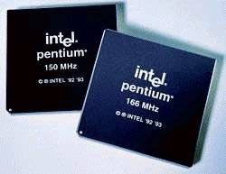
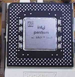
Pentium Classic (P54C)This chip was developed by Intel in Haifa, Israel and was released on March the 22th 1993. The Pentium processor is super scalar, meaning that it can execute more than one instruction per clock tick. Typically, it handles two instructions per tick. In this respect, we can compare it to a double 486. At the same time there have been big changes in the system bus: the width is doubled to 64 bit and the speed is increased to 60 or 66 MHz. This results in a substantial improvement from the 486 technology. Originally, Pentium came in two versions: a 60 MHz and a 66 MHz. Both operated on 5 Volt. This produced a lot of heat (it was said that you could fry an egg on them!) The next Pentium (P54C) generation had a built in 1½ clock doubling, and ran at 3½ Volt. This took care of the heat problem. Since then, Intel carried two Pentium lines: those which run at 60 MHz on the system bus (P90, P120, P150, and P180) and the rest, which ran at 66 MHz (P100, P133, P166 and P200).
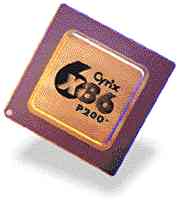
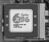
Cyrix
|
|
|
|
|
System bus speed |
| P120+ | 100 MHz | 2 | 50 MHz |
| P133+ | 110 MHz | 2 | 55 MHz |
| P166+ | 133 MHz | 2 | 66 MHz |
| P200+ | 150 MHz | 2 | 75 MHz |
An interesting detail was, that the 6X86 P200+ was the first CPU to run a system bus speed above 66 MHz. However it was difficult to find mother boards with chip sets capable of this, so the chip never achieved an important position in the market.
Cyrix 6X86s were known for poor performance regarding floating point operations. There also were problems with Cyrix and NT 4.0. In my experience, the 6x86 did quite a good job with common office programs in Windows 95. I was very satisfied with the P166+ I had. Of course I would prefer a genuine Pentium 166, but I was not willing to pay three times the price at that time.
The 6X86 has later been improved with Dual Voltage (like Pentium P55C). This reduces power consumption and heat generation.
AMD is another CPU brand. Their Pentium like chips offer Intel tight competition. AMD use their own technologies Therefore, they are not clones. They have these series:
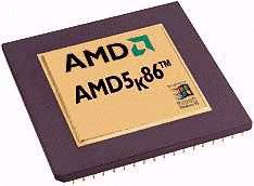
AMD's K5 also existed as PR166. As the name suggests, it was intended to compete with Intel's P166. It operated at just 116.6 MHz internally (1.75 X 66 MHz). According to the highly respected German magazine c't, issue 3.97 page 20, it actually ran at least as fast as the P166.
This was due to an optimized cache and other new developments. The only feature on which it could not match the P166 was in floating point operations. These are typically necessary in 3D calculations in AutoCAD and similar applications.
PR133 and PR166 cost far less than the similar Pentium models, and they
were very popular in low budget machines.
The P55C Pentiums were introduced January 8, 1997. MMX is a new set of instructions (57 new integer instructions, four new data types, and eight 64 bit registers), which expand the capabilities of the CPU. It is an addition to the original Pentium set of instructions.
The MMX instructions were designed for multimedia programs. The programmers can utilize these instructions in their programs. These allow the Pentium to provide improved program execution.
Both Cyrix and AMD use MMX in their 6th generation CPUs (K6 and M2). Programs, which are written with MMX instructions, can still be run on, for example, a Pentium without MMX. However, execution is slower with the traditional instructions.
IDT is a smaller company producing low-priced Pentium MMX-like CPUs. Their first WinChip C6 was introduced in May 1997. The company wanted to deliver 200 MHz Pentium MMXs for $50.
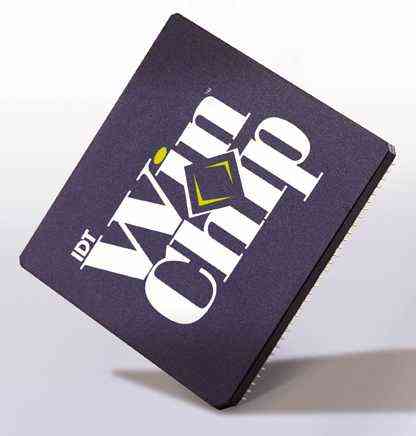
About the IDT WinChip C6 CPU:
Check the IDT WinChip web for more information.
One of the newest CPU technologies is the continually thinner wires inside the chip. With thinner wires, the CPU can operate at lower voltage. That results in a smaller CPU generating less heat and with the ability to operate at higher speeds. A step in this development is the design of dual voltage chips:
| CPU | Internal voltage | I/O voltage |
| Pentium MMX | 2.8 Volt | 3.3 Volt |
| AMD K6 | 2.8/2.9 Volt | 3.3 Volt |
| Cyrix 6X86MX | 2.8 Volt | 3.3 Volt |
| Pentium II "Klamath" |
|
|
| AMD K6-2 |
|
|
| Pentium II "Deschutes" |
|
|
It takes a long time to manufacture a CPU. 5 to 10 million transistors must be placed on a tiny silicon wafer. Actually, it required 90 workdays 24 hours round-the-clock to produce a Pentium CPU.
CPUs are manufactured in large wafers containing 140 to 150 CPUs. Usually 110 to 120 of these perform perfectly. The rest are discarded. The wafers are burned, etched, and treated in hour long processes - layer by layer. In the CPU there are up to 20 layers of silicon wafers with millions of micro transistors.
| CPU | Process technology | Number of transistors | die size |
|
|
1.0 micron |
|
|
|
|
0.5 micron |
|
|
|
|
0.5 micron |
|
|
|
|
0.35 micron |
|
|
|
|
0.25 micron |
|
|
|
|
0.35 micron
0.25 micron |
|
|
|
|
0.25 micron |
|
|
|
|
0.25 micron |
|
|
|
|
0.25 micron |
|
|
|
|
0.25 micron |
|
|
Here you see the Intel process generations:
| Process generation | Year | Gate length |
|
|
1989 |
|
|
|
1991 |
|
|
|
1993 |
|
|
|
1995 |
|
|
|
1997 |
|
|
|
1999 |
|
The CPUs have doubled their calculating capacity every 18 months. This is called "Moore's Law" and was predicted in 1965 by Gordon Moore. He was right for more than 30 years. The latest CPUs use internal wiring only 0.25 microns wide (1/400 of a human hair). But if Moore's Law has to be valid into the next century, more transistors have to be squeezed onto silicon layers.
And now there is a new hope. IBM has for the first time succeeded in making copper conductors instead of aluminum. Copper is cheaper and faster, but the problem was to isolate it from the silicon. The problem has been solved with a new type of coating, and now chips can be designed with 0.13 micron technology. The technology is expected later to work with just 0.05 micron wiring!
Texas Instruments announced on August 27th 1998 that they expect 0.07 micron CMOS processing in the year 2001.
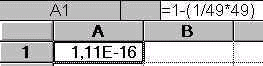
The following miscalculations occur in 386, 486, and Pentium, when running Excel, Works, or Pascal, with the numbers 49 and 187:
All CPUs have faulty instructions. Recently flaws have been discovered within the Pentium II and Cyrix 6x86MX.
Pentium was hit by a scandal in late 1994, when an error in the mathematical co-processor (FPU) became publicly known. It simply miscalculated at a given division. Intel knew of the error from early that summer but more or less kept it secret.
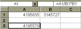
Intel insisted that the error would occur extremely rarely. Compaq immediately modified their production to disable the FPU. Shortly thereafter, IBM announced that they would stop the production of Pentium based PCs. IBM had calculated that the error would occur every 24 days. At the time, IBM was working to extricate themselves from the Intel CPU monopoly. They were moving towards Power PC, Cyrix, and NexGen based PCs. Thus the scandal played right into their hands. You see the error here, where A3 should be equal to A1:
Intel underestimated the significance of the miscalculations, certainly regarding users employing complex mathematical calculations. IBM over dramatized the error for political reasons. This all happened in December 1994, while Intel was running their big TV campaign for Pentium.
That gave birth to a number of jokes: How many Pentium programmers are needed to screw in a bulb? (answer: 1.9990427). Why is Pentium not named 586? Because it would have to be called 585.999983405! In a different vein: How many Apple employees does it require to change a bulb? 7! One to hold the bulb and 6 to design T-shirts. And: how many IBM employees does it require to change a bulb? None! IBM simply announces a new feature called "black bulb."
In 1997 a total of 100 million CPUs of the x86-family was sold worldwide. Intel held 85% of this market.
This site is good if you are interested in the CPUs. The Intel Owner's Club is a free, easy way for members to:
![[ Go back ]](prev.gif)
![[ Go next ]](next.gif)